Authored by Shen-Li Chen*,
Abstract
High holding voltage of the stacked circular ultra-high voltage (UHV) nLDMOS component with slightly lowered ESD ability is developed by a TSMC 0.5-μm Bipolar-CMOS-DMOS (BCD) process. The holding voltage is an important parameter concerned with the latch-up immunity in a CMOS IC. In general, the holding-voltage value of a traditional nLDMOS is much lower than the supply voltage (VDD), there has high latch-up risk. In this paper, a stacking architecture of nLDMOS transistors is used to investigate the ESD ability and latch-up immunity. From experimental results, as three nLDMOS DUTs were stacked, this component has a highest holding voltage up to 180.59-V and a relatively vigorous ESD capability under without altering the operating voltage of the DUT.
Keywords: Electrostatic discharge (ESD); Holding voltage (Vh); Latch-up (LU); Lateral-diffused MOSFET (LDMOS); Transmission-line pulse (TLP); Ultra-high voltage (UHV)
Introduction
Electrostatic discharge issue has been an important factor impacting the reliability of ICs in ultra-high voltage (UHV) applications, which makes UHV ICs pose serious risk of ESD damage [1-6]. Therefore, ESD protection techniques have been emphasized to improve the reliability in UHV usages. Moreover, an UHV LDMOS has been widely implemented in power electronics and power management circuits. Of course, an LDMOS is often used as an ESD protection device [7-9]. However, the ESD ability of LDMOS is very poor due to the current crowding effect, which makes the local power of a device too high to cause device melted [1], [10,11]. Furthermore, when the applied voltage is sufficient to trigger the parasitic BJT of an nLDMOS turned-on, a snapback effect occurred, and the minimum voltage to maintain the parasitic BJT conduction called the holding voltage. Under a normal operation, when the holding voltage lowers than supply voltage VDD and there is an external noise triggering this parasitic BJT of nLDMOS, the parasitic device will be turned on and finally caused the device to overheat (failure). However, the device stacked skill has been used to improve holding voltage in LV and HV applications [12-14] but seldom exercised in UHV fields. Although the Reference device has commercially sufficient ESD abilities by our design, but its holding voltage is too low and therefore poses a serious latch-up risk. In this paper, the holding voltage has been promoted through the devices stacked under keeping the variation small of breakdown voltage and is realized via a TSMC 0.5-μm BCD process.
Layouts of UHV Circular nLDMOSs Components
Reference device of UHV circular nLDMOS
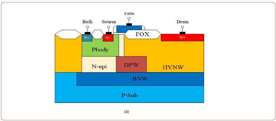
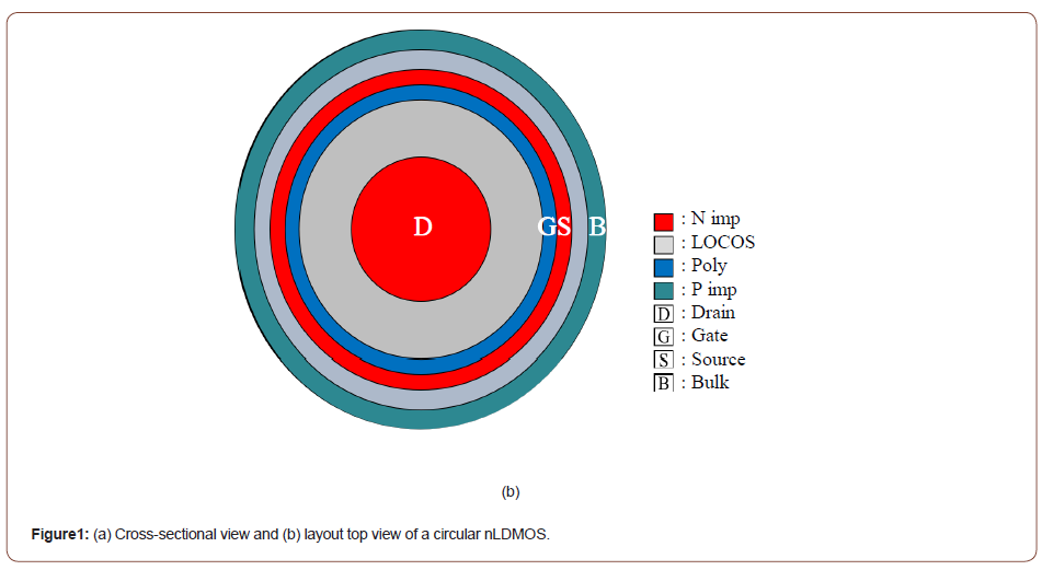
The cross-section view and layout top view are shown in Figure 1(a) and 1(b), respectively. Due to the operation voltage of UHV applications, there are some technologies being used to upgrade the breakdown voltage of DUT. First of all, a field oxide layer (FOX) is fabricated upon the drift region to reduce the peak electric field. Next, an n-lightly doped HVNW layer is used in the drift region to increase the junction breakdown voltage. Final, the P-body and the deep P-Well (DPW) form a RESURF structure, which causes the drift region to be completely depleted and increases the junction breakdown voltage of the DUT without increasing the length of the drift region. Usually, an UHV ESD protection device adopts the elliptical or circular layout types to avoid sharp-edge effects which will cause an UHV device easily to fail. In this paper, a circular layout type is used, which can reduce the layout area but also make the electric-field distribution more uniform. A semiconductor curve tracer is used to measure the I-V curve and breakdown voltage to assure that the device has correct characteristics. The device configuration in this work forms a gategrounded nMOSFET (GGnMOS) structure so that an ESD transient current can be dissipated through the beneath parasitic BJT. All of devices in this work have the same channel length (4μm), channel width (263.26μm) and drift region (5.8μm).
Device stacking modulation of UHV circular nLDMOSs
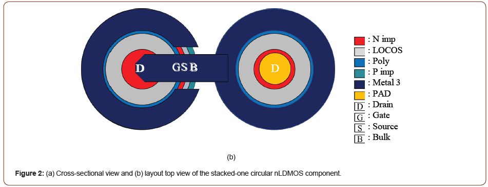
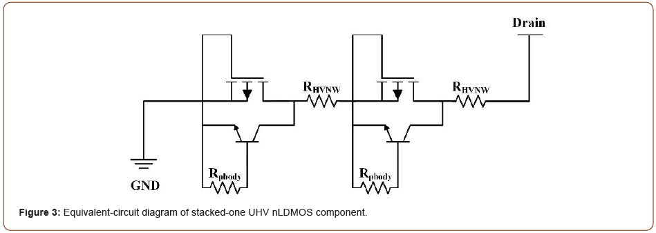
The cross-section view, layout top view, and schematic equivalent-circuit diagram of stacked-one device are shown in Figure 2 and 3, respectively. By stacking one, two and three devices, the relationship between holding voltage and secondary breakdown current can be evaluated. A stacked device can increase the current path which also increases the equivalent series resistance, so that the holding voltage can be increased. Since the operating voltages of UHV devices are much higher than the LV devices, considering the reliability of these stacking devices, the metal-3 connection between two stacking devices was used in order to prevent a parasitic device under metal line turned-on. Meanwhile, for maintaining the operation voltage of the circuit, the stacked gap between these two UHV transistors has been well designed to keep the breakdown-voltage variation small of these stacked DUTs.

Testing Method and Testing Machine
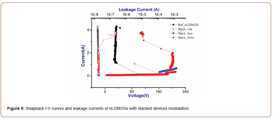
In Figure 4, a transmission-line pulse testing machine (TLP) is used and it can achieve an automated measurement process via the LabVIEW software. This tester provides a continuous rising square waveform with 100 ns pulse width and a short rising/falling time of <10 ns to obtain I-V data responses through the devices. This short transient pulse is used to simulate the HBM waveform of an ESD event. The I-V characteristics of these devices, such as the trigger voltage (Vt1), holding voltage (Vh), and secondary breakdown current (It2) can be measured.

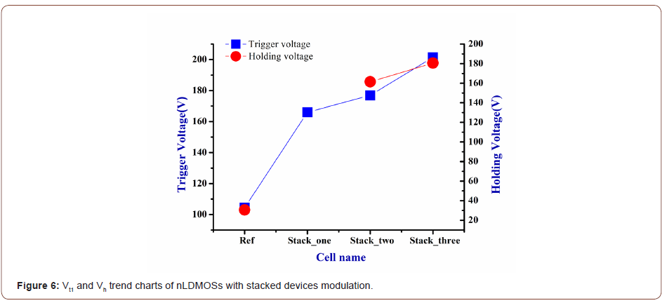
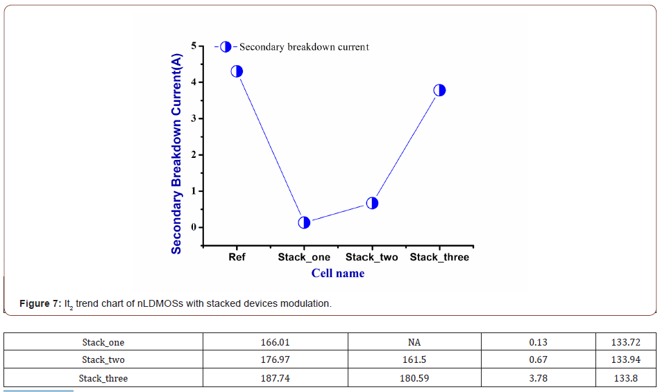
architectures are shown in Figure 5-7 and Table 1. These data demonstrated that the It2 value (directly related to ESD capability) of Reference DUT can up to 4.3 A, but the Vh value is far less than the supply voltage, so that the latch-up risk must be considered. For the stacked-one component, due to the device structure is asymmetric and the contacts number at source-/bulk-side (especially for the inner source-side zone) is far less than drain side, this DUT failed immediately (due to higher Vh of this stacked component) after parasitic BJTs had triggered so that its holding voltage cannot be measured. Next, for the stacked-two component, higher the equivalent series resistance and resulting in the lower ESD transient current. And then, higher the Vh and It2 values of this stacked-two component. And, as for the stacked-three component, because more devices shared the voltage, then the parasitic BJT turned-on when the voltage reached 187 V. Obviously, more the stacked devices to disperse the applied voltage, eventually, the holding voltage of this high stacked number component will be higher than 102 V so the latch-up immunity substantial increased; meanwhile, the It2 value (ESD capability) of this component does still perform quite well due to the ESD-sharing effect.

Conclusion
In this paper, the stacked-devices technique for the UHV application is successfully realized for increasing the holding voltage and maintaining good enough ESD ability for the circular UHV nLDMOS. In the stacked-three component , due to the suitable series devices number, the holding voltage can be increased from 30.56 V to 180.59 V without altering the operating voltage of the DUT, meanwhile it can maintain high enough ESD ability.
To read more about this article...Open access Journal of Modern Concepts in Material Science
Please follow the URL to access more information about this article
To know more about our Journals...Iris Publishers
To know about Open Access Publishers


No comments:
Post a Comment